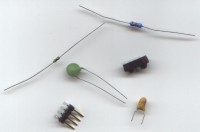
You will also need some strip board or make up a PCB. My first
IrDA connectors were mad on strip board, but I have recently experimented
with making PCBs. I hear you say "but I need really expensive kit to
do that!" and "it'll cost a fortune!". Well that is not the
case. I got a Student
Etch Pack from Maplin' for £17.99 and it had almost everything I
needed.
The process I used can be found here.
It is a very good guide and talks you through the process of using a standard
laser printer to make the tracks on your PCB. I have had success with Epson'
Photo Paper (S041140) and Kodak' Inkjet Photo Paper (CAT 819 6743). I found
that using 400 grit wet'n'dry paper was the best to prepare the board. Any
finer and the toner will not stick very well and coarser it will score the
board deeply. Another thing I noticed was that the Kodak paper blisters on
the reverse side so put a piece of plane paper between the iron and the photo
paper.
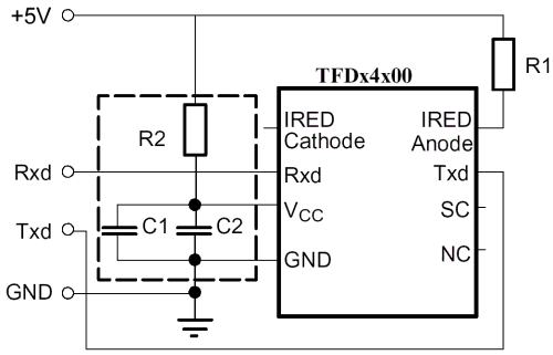
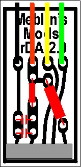
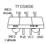
First it was necessary to work out how to put the components
together? The data sheet for the TFDS4500 provides a simple schematic to enable
you to construct a circuit from. I have adjusted it slightly to simplify it
to our needs.
R1 is the 13W 0·25W Metal
Film Resistor and R2 is the 47W 0.125W Metal Film
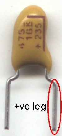
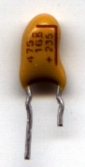
Resistor. It doesn't matter which capacitor you put in C1 and C2, but you
must make sure that the +ve leg of the Tantalum capacitor is at the node junction
with R2.
Initially I used strip board and used wires when
I needed to link between the sets of holes. However, this meant that the TFDS4500
was on the opposite side to the rest of the components. So, after a little
thinking, I came up with a way to place the components on a PCB.
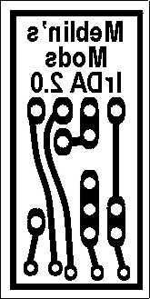
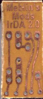
Strip Board Original
PCB
(click the image for a full size
template)
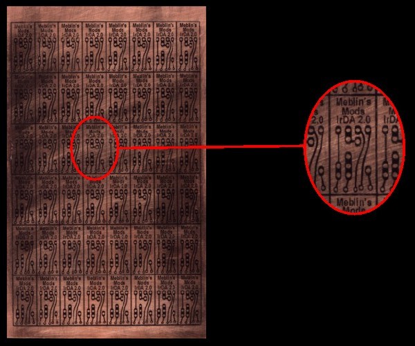
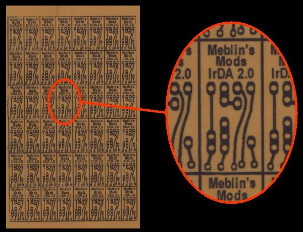
Once I had perfected the design, I was able to print a load
onto my photo quality paper to allow me to transfer the toner to the copper
clad board. I had my iron set just above half way and made sure it was up
to temperature before I printed the design. It's very important to do the
ironing stage as quickly as possible once the design has been printed.
I placed my board on the ironing board (copper side up), put
the design face down on the copper face, placed a blank piece of paper over
the photo paper and began to iron making sure I applied lots of pressure.
I probably ironed for about 5 minutes, making sure that I pressed all over
firmly. You can lift a small corner to see how well it is working. I then
ran it under cold water for several minutes. If you leave it for ages it will
become a pulp. I just kept testing to see if it would lift away with ease.
This will leave you with this result:
Next is the boring part of waiting for the etch
to work. Being winter, this process took about 2 hours and you should end
up with something like this:
Next is another boring part, drilling the holes!!!!!
Well my drill was flat and the charger has gone AWOL so I whipped out my hand
drill and started to drill all the holes. The larger holes are 1mm and the smaller
ones are 0.8mm. This took a fair while and I managed to break my 1mm drill bit.
Don't press to hard! I did manage to get a chuck for my dremel-a-like to drill
the 0.8mm holes. It made light work of that!
Once the board had been drilled I uses some wet'n'dry
paper to remove the toner, making sure not to break the tracks accidentally,
and cut it into little boards with a craft knife.
Now onto the fun part.
You may be wondering why I have only created 5
holes for the TFDS4500 when it has 8 pins? Well the answer is simple; 3 are
not needed. Therefore, I carefully snap off the SC, NC and IRED Cathode legs
along with the 2 supporting pins at either end. It's then necessary to straighten
the legs so that they will pass easily through the holes. The it's just a case
of soldering the legs to the copper tacks, being careful not to create solder
bridges between adjacent tracks.
It is also necessary to straighten and shorten
the Tantalum capacitor legs, to enable them to fir into the holes, and trim
the other capacitor and resistors once they had been soldered into place..
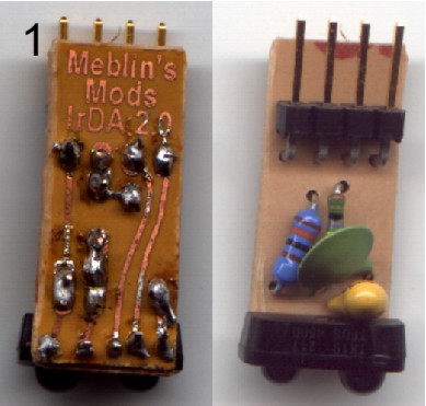
Once complete your final IrDA receiver/transmitter
should look like this:
If the etching process was a little harsh on your
tracks, the easy way to fix it is to heat the track up and use solder to link
over the gap (remember solder is attracted to heat). On the track that goes
to the 2nd pin from the right, you can see how this would work (this was an
overspill of solder from the join of the 13W. Honest!!!!)
The next step is to make up a cable to connect
the device to your motherboard header. I have used the housing and crimp terminals
from RS. However, you can only but the terminals in packs of 100 for £9ish.
Maplin do an alternative PCB Terminal and Socket Housing (YW25C
& HB58N)
for alot less and smaller quantities, but I have found the RS version easier
to work with.
First of all you need to strip the outer sleeve
and screening wire to about 15-20mm. You will then find that you have 4 different
coloured wires. RED, Blue,
YELLOW and GREEN. I use the RED
for the 5V connection, BLUE for gnd, YELLOW for
RxD and GREEN for TxD. Once you have decided on
your colour scheme, strip the wires to about 5-7mm, place in the crimp terminals
and then crimp the terminal aroung the wire. This is quite tricky and takes
a few goes to get it right. I tend to solder the wire slightly lower that the
crimp section to ensure the wire will not detach itself when the cable is pulled
to remove it from the motherboard.
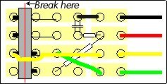
Once all 4 wires have been attached
to terminals, it's time to place them in the housing. They shoulc slot in nicely
and the order to put them in is BLUE (pin1) - RED
- YELLOW - GREEN. It is then necessary to dig out
your motherboard manual and find out what the configuration of the header is.
Just make sure you put BLUE - GND,
RED - 5V,
YELLOW - RxD and GREEN - TxD.
Some motherboard headers have 5 pins, with one plank slot on the housing, and
some are even in 2 rows. Just make sure you get it right or it will not work.
Once that is done you need to change
your BIOS settings to enable IrDA. This feature will usually knock out one of
your serial ports (if you have 2). So if you have 2 serial devices you may only
want to enable this option when you are downloading/uploading stuff to your
IrDA device. When you log into Windows you will be prompted to install a new
device so have your windows disks handy. That's all there is to it. When an
IrDA device is near by (in win2K any way) you will hear a ZAP noise and in the
system tray an infrared signal icon will appear. You can get loads of software
to upload stuff to phones. Nokia do one to save all your numbers, etc...
If you are using win 98 it's a
little more complex to get a conection between, say, a laptop and your puter,
You will need to set up a direct connection.
Well I hope you kept up and have
fun. For those of you that are too lazy to DIY the click the linkl below to
by one to order.